

TL;DR
- Two numbers on a GPU spec sheet set the limits on how fast your work can run: peak FLOPs and peak memory bandwidth. Which of the two is holding you back depends on how much math your workload does per byte it moves.
- On the H100, H200 and B200 sheets the headline Tensor Core figure is footnoted with sparsity, so the dense figure is half of it. Divide the printed number straight into bandwidth and you put the crossing in the wrong place by a factor of two.
- Peak FLOPs divided by peak memory bandwidth gives the ridge point, the value of arithmetic intensity where the memory ceiling hands over to the compute ceiling. Work it out dense, at the precision you run, and it tells you which ceiling your traffic sits under.
- In this piece we walk through what the ridge point is, how to read the compute figure NVIDIA prints, and the ridge points of the H100, H200 and B200. Then we cover why decode sits far below all of them, and what the roofline cannot see.
What is the ridge point of a GPU?
The ridge point of a GPU is the amount of math per byte at which the limit on your workload stops being the memory system and starts being the arithmetic. It comes out of the roofline model, which bounds what a workload can attain from three things: the machine's peak floating-point performance, its peak memory bandwidth, and the arithmetic intensity of the application. Two of them are properties of the GPU you are buying. Peak FLOPs and peak bandwidth are fixed in the silicon and settled during chip design, so nothing you do to the workload will move them.
The third input, arithmetic intensity, is the number of floating-point operations a piece of work performs divided by the bytes it has to move to support them. It is math done per byte moved, and it is the only one of the three inputs your own code controls.
The two hardware ceilings cross at one value of arithmetic intensity, where the sloped bandwidth ceiling meets the flat compute ceiling at peak FLOPs divided by peak memory bandwidth. NERSC calls that crossing the "machine balance" point, which most people call the ridge point. Because the division is a rate over a rate, the seconds cancel and leave a count of operations per byte.
Which side of the ridge point your work falls on tells you which ceiling is binding. A workload below the ridge point is usually held back by the memory system, so a part with higher peak compute and the same bandwidth will not run it any faster. Above the ridge point, the limit is more likely to be how fast the computation can be done. The ridge point is an input to that diagnosis rather than the diagnosis itself, because a published peak is a ceiling and not a speed any workload reaches.
The number NVIDIA prints is twice the one you want to divide
In the H100 SXM column of NVIDIA's H100 product page, the BFLOAT16 Tensor Core row reads 1,979 teraFLOPS and the GPU memory bandwidth row reads 3.35 TB/s.
The Tensor Core row carries an asterisk, and the footnote under the table reads "With sparsity". So 1,979 teraFLOPS is the ceiling for a workload with sparsity. The dense ceiling applies to a workload that is not sparse, and it is half of that figure, 989.5 TFLOP/s.
Divide 989.5 TFLOP/s by 3.35 TB/s, and the answer is about 295 FLOP per byte on the SXM part at dense BF16, by our own arithmetic. Use the printed 1,979 instead, and the result is about 590. That sets a sparse ceiling against a dense workload and puts the crossing in the wrong place by a factor of two.
One row away on the same page, the TF32 Tensor Core row reads 989 teraFLOPS, also with sparsity. Those digits are a coincidence, because the row is a different precision. It is not the dense BF16 figure you have just worked out.
The page also prints a second column, for the H100 NVL, and its compute and bandwidth figures both differ from the SXM ones. So a ridge point built from one number in each column belongs to no part that exists. Take both figures out of the same column.
The same division runs on any spec sheet, as long as the basis does not move
The H200 product page prints the same 1,979 TFLOPS on its BF16 Tensor Core row, footnoted with sparsity, and 4.8 TB/s of memory bandwidth. NVIDIA's Blackwell datasheet gives the B200 4.5 petaFLOPS of FP16/BF16 Tensor Core throughput and 7.7 TB/s of memory bandwidth. Its footnote puts all Tensor Core numbers except FP64 with sparsity, so the dense compute figure is 2.25 petaFLOPS.
| Part | Peak compute, dense BF16 | Peak memory bandwidth | Ridge point |
|---|---|---|---|
| NVIDIA H100 SXM | 989.5 TFLOP/s | 3.35 TB/s | about 295 FLOP per byte |
| NVIDIA H200 SXM | 989.5 TFLOP/s | 4.8 TB/s | about 206 FLOP per byte |
| NVIDIA B200, HGX | 2,250 TFLOP/s | 7.7 TB/s | about 292 FLOP per byte |
The compute and bandwidth columns come from the NVIDIA H100 and H200 product pages and the Blackwell datasheet as they stood on 1 September 2026. Each Tensor Core figure is halved to its dense value, and the ridge-point column is our division. NVIDIA marks the H200 and Blackwell tables as preliminary specifications that may change.
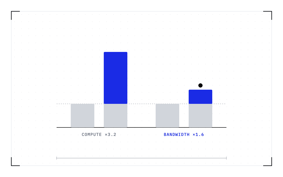
The H200 row shows most clearly that the two ceilings move independently. It publishes the H100's compute figure alongside more bandwidth, so its ridge point falls and the crossing moves left. A workload therefore needs less math per byte on an H200 than on an H100 before compute becomes the binding limit.
The B200 raises both ceilings instead. Against the H100, compute rises by 2.27 times and bandwidth by 2.30 times. The two scaled together, so the B200's ridge point lands within a few FLOP per byte of where the H100's sat. That is why a newer part is not automatically further to the right.
Every figure in the table is a published peak rather than a measured one. Vendor specifications are a good starting point for the two ceilings, and for a closer reading of what a machine attains in practice NERSC recommends the Empirical Roofline Toolkit.
Decode sits far below every ridge point in the table
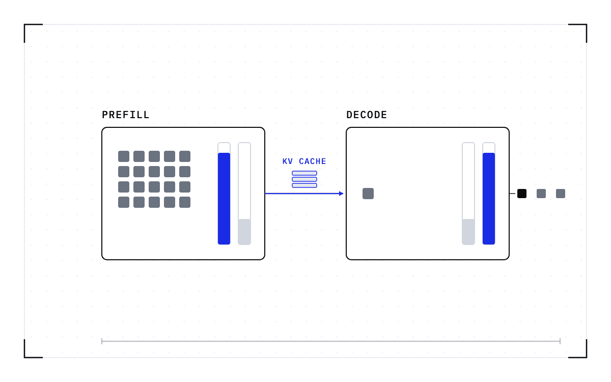
Inference has two phases, prefill and decode, and they land on opposite sides of the crossing. Prefill pushes many tokens through the model at once as large matrix multiplies. It does plenty of math per byte of weights loaded, so it sits well up the compute-bound side.
Decode produces one token at a time. It streams the full weight matrix out of high-bandwidth memory (HBM) to do a vector's worth of work. That is one sweep of the weights per token and very little math for the bytes moved. So decode sits far below every ridge point in the table.
All three parts therefore give the same answer for decode, which is that the memory ceiling is the binding one. The column that separates them is memory bandwidth.
Should I just buy better GPUs instead?
That depends on which of the two ceilings your traffic is already under, and the ridge point, set against your traffic's own arithmetic intensity, is what tells you. So compute it for the part you have and for the part you are considering, at the precision you run in production and with both compute figures dense. Do that before you compare anything else on the sheet.
The cheaper part with the lower ridge point can win on a decode-heavy workload. The ridge point alone does not rank parts, because your traffic mix, the precision you run and the price do that, and the table above is one input to it.
The roofline assumes the GPU is already serving
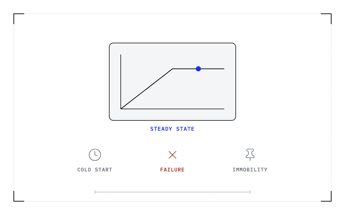
The roofline bounds one kernel on one device in steady state. It presumes the weights are already resident and the GPU is already answering requests, so the graph shows neither the time before serving begins nor the time after it stops.
The ridge point settles which ceiling your traffic sits under while the part is serving, and it says nothing about the minutes that part spends loading a model or recovering after a node fails.
Those minutes are what we work on at Cedana. Cedana is automated GPU checkpointing and migration infrastructure that increases the useful work your GPUs deliver. We save the whole state of a running workload and bring it back on the same or different hardware, so a start becomes a restore and a failure becomes a resume. When you size your next batch of GPUs, the ridge point tells you what a part can do while it is serving, and the hours it spends not serving are a number you have to count separately.